WE CAN NOT BUILD THE FUTURE OF ANGSTROM-
ERA SYSTEM-ON-CHIP (SOC) WITH METHODS CREATED IN THE MICRON ERA.
COMPANY
VegaSemi develops next-generation technology for the angstrom era, overcoming the limits imposed by today’s heavy AI computation.
As AI systems drive chip power toward multi-kilowatt levels and push data centers toward a global “power wall,” our unified adaptive architecture enables silicon to operate at its true minimum safe voltage—even under extreme AI workloads—while delivering complete security, reliability, and in-field test solutions, all governed by a single intelligent control loop.
We build silicon that continuously adapts, safeguards, and optimizes itself.

TECHNOLOGY
Modern SoCs are being pushed to their limits. AI/ML workloads are driving power consumption toward the physical power wall, while autonomous driving, robotics, and other mission-critical systems demand far tighter safety margins than ever before. At the same time, advanced FinFET and scaling technology nodes age faster and behave less predictably, making long-term reliability a central concern.
Security has also become a defining constraint. Attack techniques have grown increasingly sophisticated, and their impact on emerging technologies is profound—directly affecting the trustworthiness and functional integrity of safety-critical systems like autonomous mobility and industrial automation.
Yet today, the industry still approaches these challenges in a fragmented and siloed way. Each problem—power, security, safety, and reliability—is handled separately, resulting in limited performance gains, added complexity, and systems that struggle to operate cohesively.
Today’s solutions are rooted in the past. They were built for an era when these issues could be treated as independent domains. But the complexity of modern AI platforms, autonomous systems, and advanced scaling technologies has outgrown this mindset. The industry now needs a true paradigm shift in SoC design—one where these challenges are addressed through a unified, intelligent framework operating continuously in real time.
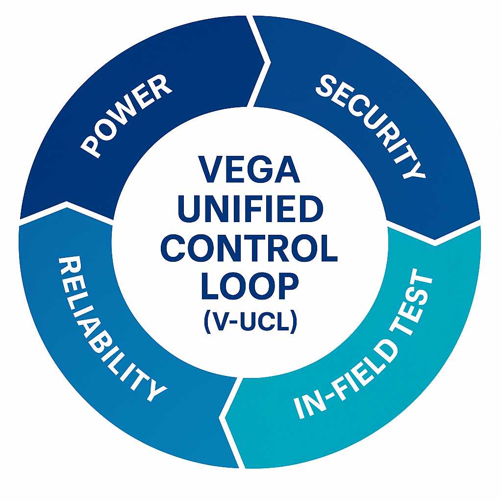
This is the philosophy behind VegaSemi’s unified approach, where power integrity, security resilience, in-field test, and long-term reliability work together cohesively rather than as disconnected subsystems. It is a foundational shift in how modern silicon is designed, monitored, and safeguarded throughout its lifetime.
VegaSemi develops a unified silicon-control architecture that brings together power management, reliability monitoring, security protection, and in-field test into one cohesive system. Instead of treating these functions as separate subsystems, VegaSemi integrates them into a single intelligent loop that continuously adapts to real workloads, environmental conditions, aging behavior, and potential fault or attack scenarios. This unified approach enables highly efficient, resilient, and predictable operation across AI accelerators, cloud and edge platforms, automotive systems, and advanced high-performance SoCs. This cohesive control system represents a true paradigm shift in how modern SoCs are architected and maintained.
The four pillars below represent the foundation of VegaSemi’s technology for the angstrom era.

⚡ POWER
Operate at the true minimum safe voltage—under every workload.
VegaSemi delivers true fine-grain DVFS using a novel, programmable, and precise margin-sensing technique that determines the real minimum safe voltage (Vmin) of each core under its actual operating conditions.
This eliminates heavy chip characterization, calibration data storage, and large voltage tables. The system dynamically tracks temperature, workload stress, and long-term aging to maintain the correct minimum safe voltage throughout lifetime.
And thanks to VegaSemi’s zero-latency voltage-droop detector with same-cycle correction, Vmin is fully protected so each domain can operate at maximum efficiency without compromising stability.
🛡️ SECURITY
Miniaturized, distributed sensors for attack-resilient silicon.
VegaSemi engineered the industry’s most compact supply-droop and clock-glitch sensors, with extremely small area overhead enabling wide distribution across the SoC.
These miniature sensors detect malicious disturbances—including EM pulses, laser injection, undervolting attempts, clock manipulation, and abuse of DVFS activity—and also mitigate their impact in real time, keeping systems stable even under attack.
A distributed sensor network provides continuous spatial coverage and streams detailed anomaly data to firmware or system software, enabling deep threat forensics and improved long-term security for mission-critical electronics.
♾️ RELIABILITY
Lifetime reliability assurance.
VegaSemi delivers intelligent lifetime-margin monitoring technology that ensures long-term performance stability. As aging becomes a major limiter in advanced silicon nodes such as 5 nm, 3 nm, and 2 nm, today’s industry—especially in safety-critical applications— responds by adding 10–15% lifetime guard-bands to cover uncertainty.
This forces chips to operate above their true voltage needs for most of their lifespan, wasting power and accelerating aging, which further shortens device longevity.
VegaSemi’s reliability architecture provides continuous awareness of how silicon evolves under real operating conditions and intelligently tunes lifetime margin over years of operation. This maintains predictable timing behavior without the heavy guard-bands typically required to compensate for aging drift.
The result is long-term performance stability, improved energy efficiency, and the system-health insight required for high-reliability, long-lifetime applications across automotive, AI, data-center, industrial, and aerospace markets.
🔍 IN-FIELD TEST (IFT)
Continuous in-operation test and safety monitoring.
VegaSemi delivers cutting-edge In-Field Test technology that provides continuous in-operation test, health monitoring, and lifetime safety oversight.
VegaSemi’s IFT architecture runs seamlessly during normal system activity with no test mode, no scan interruption, minimum vector storage, and no performance loss. By avoiding testing the chip only during start/stop events or idle periods, IFT captures real silicon behavior under true workloads and true PVT conditions throughout the entire mission profile.
IFT continuously tests the system to detect failures as they begin to develop, identifying faults, degradation, abnormal behavior, and early signs of silicon drift while applications run normally. Furthermore, VegaSemi technology enables validation of DVFS and aging-compensation adjustments, supports predictive maintenance and safety certification, and allows long-term silicon-health analysis.
IFT is also fully compatible with critical-mission safety frameworks such as ISO 26262 and ISO 21434, ensuring that monitoring and diagnostic coverage requirements are continuously met throughout operation. This in-operation testing facilitates intelligent workload balancing across compute clusters, distributing stress evenly and extending silicon lifetime in automotive, AI, and high-availability systems.
The technique can drastically improve failure analysis by allowing test and reliability teams to evaluate the chip directly on the board, significantly reducing the cost and impact of RMAs. IFT can also be leveraged during manufacturing test to reduce overall test time and lower production test cost.
NEWS
No new news at this time.
CONTACT
For partnerships, technical discussions, or investment inquiries, please reach out:
Email: contact@vegasemi.com
Location:
9191 Towne Centre Drive, Suite 150
San Diego, CA 92122
